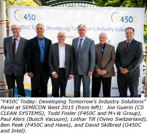
Ben Peek began his career as a research chemist with Texas Instruments, R&D Labs, in the 1960s. His interest was surface chemistry (flat surfaces) and basic research in exotic semiconductor materials such as gallium arsenide (GaAs), germanium, indium phosphide (InP), indium antimonide (InSb), and mercury cadmium telluride (HgCdTe). These materials are today’s mainstays for speed and for building sensors. After the research role, Peek began operating pilot production lines in TI’s early product portfolios for microwave devices, digital signal processing components and integrated circuits. Later, Peek was involved in early high performance computing activity primarily focused on signal processing, a major area of interest for most of his career. From building devices in a fab, he focused on applications such as processing seismic data, radar data, and space based infrared data. While maintaining an interest in signal processing through many sensor technologies, today he is the Haws F450C architect. In this role he is responsible for Haws’ Effluent Monitoring Systems (EMS™), a collection of sensors that monitor effluent from semiconductor process tools.
Integrated circuits manufactured in future fabs running 450mm silicon wafers will require tighter specifications for Ultra-Pure Water (UPW), De-Ionized Water (DIW) and Ultra-High Purity (UHP) air. As semiconductor process technologies move beyond 22 nm, simply scaling existing fabs to handle larger wafers could lead to unsustainable construction and operational costs. State-of-the-art sensor monitoring techniques can be used in a variety of applications like fluid flows, energy consumption, and semiconductor process chemistries. This monitoring provides the analytics required to better right-size utility infrastructure in order to contain costs. Semiconductor fabs have evolved technology innovation faster than many other manufacturing technologies and are well positioned to optimize the design and implementation of sustainable factory infrastructure such that environmental risk is minimized for water, process chemicals and energy.
Traditionally, for 200mm and 300mm silicon fabs, there is evidence that supply systems have been over-designed “just to be safe”, often by a major factor. Such facilities can include oversized infrastructure for process elements including chemicals, gases, air, water and energy. Such excessive capacity may have been adequate to safely run “blind” with minimal sensors and deficient knowledge – even for 300 mm wafers. This approach will not play for 450mm wafers where issues of affordability and the volumes of process chemistries, water and energy no longer make sense using traditional design techniques. A leading 300mm fab can consume 2-4 million gallons of water per day and scaling these fab designs to process 450mm wafers could consume >8 million gallons a day. Such volumes of water would limit the location of such a fab to areas where the availability of water would make sense. Cost is clearly a major issue.
The semiconductor industry is a leader in the reduction, re-use, and recycling of process materials. Water use has been reduced in major ways for most 300mm fabs in production today. New facility monitoring technologies can be deployed to help minimize increases in water consumption for future fabs. Downstream or effluent monitoring can provide feedback on when a process tool has adequately completed a cleaning step, for example. Optimizing the amounts of water, energy and process chemicals consumed reduces the capital required to build a new fab by reducing the infrastructure that may not be fully used in some fabs today.
Author: Ben Peek
F450C Project Architect – Haws Corporation

